INSTRUCTION MANUAL
MODEL 1681
SOLID STATE ADJUSTABLE SPEED
DC MOTOR CONTROL
1681 INSTRUCTION MANUAL
TABLE OF CONTENTS
1.1 Electrical
1.2 Mechanical
2.1 Electrical
2.2 Mechanical
2.3 Environmental
3.1 Power Section & Transient Protection
3.2 Block Diagrams of DC Motor Control
3.3 Input Amplifier & Ramp Circuits
3.4 Reference Voltage
3.5 Minimum Speed Circuit
3.6 Electronic Mode Selector Switch
3.7 IR Compensation
3.8 Speed Regulator
3.9 Initial Starting Current Timer
3.10 Isolation Circuit
3.11 Firing Circuit
3.11.1 Clock (Voltage Controlled Oscillator)
3.11.2 Reference Detectors
3.11.3 Counting Circuit
3.11.4 Gate Pulse Oscillator
3.12 Fault Protection
3.12.1 Phase Sequence & Phase Loss
3.12.2 Overtemperature & Interlock
3.12.3 Current Trip
4.1 Mechanical Installation
4.2 Electrical Installation
4.3 Checks Before Initial Start-Up
4.4 Trim Adjustment Settings
- Servicing and Trouble-Shooting Procedures
- Diagrams – Tables – Application Information
General Description
- GENERAL DESCRIPTION
This manual is applicable to all integral horsepower DC motor controls of this series from 40 HP to 300 HP. The integrated circuit regulator selection of these DC motor controls are modular in construction, affording a minimum of down time in the event of a malfunction. Exceptional speed regulation and torque limiting is realized over their full operating range.
Operational features include: minimum and maximum speed adjustments, acceleration and deceleration, current limit and IR compensation adjustments. In addition, forcing and stabilization adjustments are provided for stabilizing the drive in systems with various intertials and the constants. Fault logic circuitry protects the controller from over current, phase loss, incorrect phase sequence and over temperature.
All circuitry and power components are built to withstand the vibration and handling of industrial environments.
1.1 Electrical Description
The power section of the controller is a three phase full wave bridge (six thyristors). This configuration yields full-wave six-pulse control of the motor over the entire speed range.
Thyristors, which are silicon controlled rectifiers, conduct when their gate terminal is pulsed positively with respect to the cathode. Once switched on the thyristor remains conducting until its anode voltage falls to zero. Pulsing the thyristor “on” late in the half cycle, when its anode is positive, will cause a small amount of DC power to be delivered to the motor. Pulsing the thyristor early in the half cycle will result in a large amount of power being delivered to the motor. Thyristor switching waveforms are shown in section 3.1.
A printed circuit board assembly called the firing circuit provides the pulses to gate or turn on the thyristors. Three pulses spaced 60 0 apart switch the thyristor on at the adjustable point in each half cycle they appear. When low speed is called for the pulses appear late in the half cycle. When high speed is required the pulses appear earlier in the half cycle. A full description of firing circuit operation is discus s ed in section 3. 2.
The speed regulator circuit controls the firing circuit by introducing a DC level output which is proportional to the desired speed and the error in speed due to loading.
Eight trim adjustments are located on the front of the speed regulator card. These adjustments include minimum and maximum speed adjust, current limit, acceleration and deceleration, and IR compensation adjust. In addition, forcing and stability adjustments are provided. Minimum and maximum speed adjustments trim the ends of the speed range. The acceleration and deceleration adjusts set the time it will take to reach the speed setting. The acceleration and deceleration rates are essentially linear.
The current limit adjust will provide effective torque limiting from 200/0 to 250% of the controller rating. The current limit circuit will hold armature current constant within 5% at all conditions including locked armature. Current limiting is stable under all conditions.
The IR compensation adjust will allow speed regulation of 2.5% over a 20:1 range with armature voltage feedback. The speed regulator is discussed in section 3.3.
Fault conditions which might hinder operation of the motor control are sensed by the fault circuit on the control card. This circuit will shut the motor controller down if conditions of over temperature, blown fuse, phase reversal, phase loss or extreme overcurrent are present. The cards are interlocked electrically; removing any card while the system is running will cause immediate shut down of the controller. Fault detection circuitry is discussed in section 3.4.
1.2 Mechanical Description
All assemblies are mounted on a painted steel panel with electrically conducting items mounted on insulated panels. Every assembly and part is front removable. Assemblies with heat dissipating components have been carefully designed for efficient cooling. All assembled parts use locking hardware to withstand vibration and shock from handling and shipping.
Interwiring of assemblies generally conforms to J.I.C. specifications.
Surfaces of all metal parts subject to corrosion are plated, painted or anodized depending on type of metal. Circuit boards are high quality epoxy glass with gold plated contacts and are coated with epoxy, making them highly resistant to most atmospheres and humidity conditions.
Cooling is achieved by forced air.
Specifications
- SPECIFICATIONS
2.1 Electrical
Horsepower: See nameplate
Power Input: See nameplate
Speed Range @ rated torque, armature feedback for 2.50/0 speed regulation 20:1
Speed Range @ rated torque, tachometer feedback for + 0.10/0 speed regulation *40:1
Current Limiting
Adjustable from 200/0 to 2000/0 of rated armature current. Limiting with locked armature within 50/0 of initial limit point.
IR Compensation
May be adjusted for 0 to 200/0 boost
Minimum and Maximum Speed Adjustments
Minimum speed adjustment range: 0 to 200/0 of base speed
Maximum speed adjustment range: 70 to 1150/0 of base speed
Acceleration and Deceleration Adjustments
Linear ramp acceleration and deceleration, independently adjustable from 2 to 30 seconds.
*With suitable tachometer generator
Fault and Overload Protection
System shutdown for:
Overtemperature – 80° heatsink temperature Phase loss or fuse loss
Overcurrent – Instantaneously at approximately 5 times rated peak to two minutes at 150%
Phase sequence – incorrect phase sequence
Automatic Current Limit Level – cuts back to 200% maximum if over 2000/0 more than 10 seconds
Signal Input
Manual – 1K to 2.5K potentiometer for control of zero to base speed
Programmed – 0 to 5 VDC.
Withstand Voltage: 1500 volts peak to ground or AC line, maximum
2.2 Mechanical Specifications
Dimensions: 24″H x 25″W xl01/4″D
All assemblies are front removable.
The motor control must be operated in a vertical position with power input connections at the top.
Where practical, all wiring conforms to J. I. C. electrical specifications.
Cooling: Forced air.
Approximate weight: 80 lbs.
2.3 Environmental Specifications
Maximum operating temperature around controller (in or out of enclosure) 50°C.
Atmosphere: All parts subject to corrosion are plated or coated. However, highly corrosive atmospheres may eventually cause corrosion to these parts.
Operation in up to 95% relative humidity (non-condensing) is permissible.
Theory of Operation
- THEORY OF OPERATION
3.1 Power Section
The power section is made up of three pairs of thyristors connected as shown in the simplified schematic of Figure A.
Each of the three phase voltages is connected through fast acting current limiting fuses to the common of the anode of one thyristor and the cathode of another . The cathodes of three thyristors are connected together to form the positive output of the supply. The anodes of the other three thyristors are connected together to form the negative output of the supply.
Without a gating signal, the thyristors block the flow of cur rent in both directions and there is no current in the motor armature. As a properly timed gate signal is applied to each thyristor gate, the device goes into conduction and acts like a rectifier, i. e. , it conducts as long as the anode potential is positive with respect to the cathode. When the polarity changes and the current falls below the holding current of the device, the thyristor regains’ its blocking state and will remain off until it receives another gating signal.
To achieve proper bridge control, the thyristors must be pulsed in a given sequence. Conduction always occurs in pairs, i.e. current flows from an AC line through a thyristor to the armature and back through a thyristor to another AC line.
With any conduction angle the current paths are as follows: From L1 through SCR 1, motor armature, back through SCR 4 to L2. 60° later conduction from L1 is through SCR1, motor armature, back through SCR6 to L3.
From L2 through SCR3, motor armature, back through SCR6 to L3. 60° later conduction from L2 is through SCR3, motor armature, back through SCR 2 to L1.
From L3 through SCR5, motor armature, back through SCR4 to L2. 60° later conduction is from L3 through SCR5, motor armature, back through SCR2 to L 1.
Since power is supplied to the armature six times per cycle, the ripple frequency at all conduction angles is 360 Hz. Figures Band C show typical armature voltage wave shapes at half and full speed conditions with high and low torque levels.
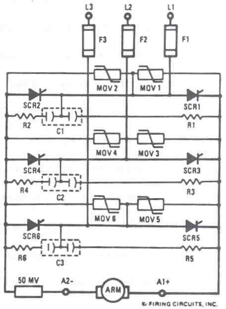
FIGURE A. 1681 DC MOTOR CONTROL.
3-PHASE FULL WAVE (6SCR) POWER CIRCUIT
TYPICAL ARMATURE VOLTAGE WAVE SHAPES
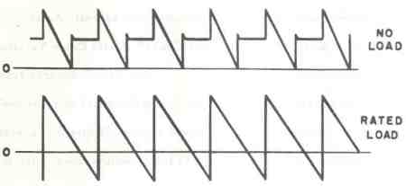
1/2 BASE SPEED
FIGURE B
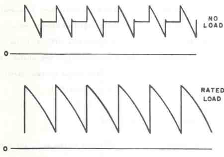
BASE SPEED
FIGURE C
3.1.1 Transient Suppression and DY /DT Protection
The power thyristors and diodes are subject to voltage transients from both the incoming power source and the output armature circuit. As shown in figure A, a series resistor-capacitor network and an “MOV” (Metal Oxide Varistor) is connected ac ros s each of the bridge SCR’s. The “MOV” absorbs transients on the lines with the help of the line impedance. Since the effect of these devices are dependent on the impedance of the AC power source, it may be necessary in some applications to add additional inductance to the incoming lines in the form of chokes or an isolation transformer.
The “MOV” device has the characteristic that it maintains a high resistance until the RMS voltage across it exceeds a certain level (well below the voltage rating of the SCR’s) I when it sharply switches to a low resistance. It recovers rapidly after the voltage level drops. The resistor-capacitor network not only serves to by pass very fast transients spikes I it also serves as a “DV/DT” buffer. “DV/DT” is the rate of rise of voltage across the semiconductor, immediately after it stops forward conduction. The buffer circuit acts to reduce the rate I giving the device more time to recover its voltage blocking characteristic.
3.2 Block Diagrams of DC Motor Control
Simplified block diagrams of the DC motor control are shown in figure 1 and figure 2. The diagrams show that the control section is isolated from the power section in both the forward and feedback paths.
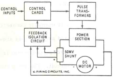
FIGURE 1. 1679/1681 DC MOTOR CONTROL.
SIMPLIFIED 8LOCK DIAGRAM
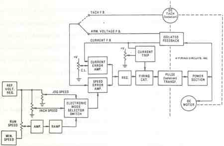
FIGURE 2. 1679/1681 DC MOTOR CONTROL.
LOGIC CIRCUIT BLOCK DIAGRAM
3.3 Input Amplifier and Ramp Circuits
The speed control potentiometer is normally connected between a five volt reference supply and the minimum speed amplifier, as shown in figure 3. The speed signal from the wiper of the control potentiometer is inverted by the input amplifier ICZ3 and fed into the ramp circuit. The ramp cirO1 it controls the motor acceleration and deceleration.
Increasing the speed setting increases the positive voltage applied to the input amplifier, causing a corresponding increase in the negative signal at the amplifier1s output. The negative signal from the input amplifier causes the output of the comparator section of ICZ8 to switch to its negative voltage limit. The negative voltage step from the comparator passes through Diode D17, and is attenuated by a voltage divider formed by the acceleration Rheostat R74 and Resistor R78. The voltage step output of the voltage divider is integrated by the integrator section of ICZ8, R 77, and Capacitor C38. The negative input step causes the output of the integrator to increase positively as a linear function of time (ramp) on a slope or rate determined by the amplitude of the input voltage step, until its positive output voltage equals the negative output voltage of the input amplifier. When the signals from the integrator and input amplifier are equal in magnitude but opposite in polarity, the comparator output will drop towards zero, and the output of the integrator will be maintained at the new speed setting.
A reduction in speed command setting reduces the input voltage to the input amplifier ICZ8, causing a corresponding reduction in the amplifierls negative output voltage. This decrease reduces the negative signal to the comparator below the positive signal coming from the integrator, resulting in a net positive signal at the comparator, causing its output to switch to the positive limit. This positive step signal passes through Diode DI8, is attenuated by the voltage divider formed by deceleration Rheostat R75 and Resistor R 78. The attenuated step signal causes the integrator to ramp in a negative direction until its output signal is equal to the new speed command.
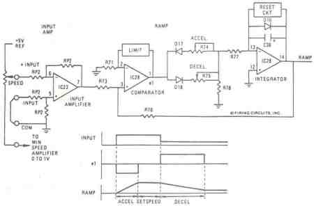
FIGURE 3. 1679/1681 DC MOTOR CONTROL.
INPUT AMPLIFIER AND RAMP CIRCUIT
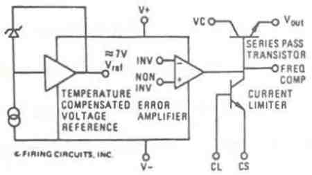
FIGURE 4A. 1679/1681 DC MOTOR CONTROL.
LOGIC CIRCUIT POWER SUPPLY REGULATOR (IC21) SIMPLIFIED SCHEMATIC
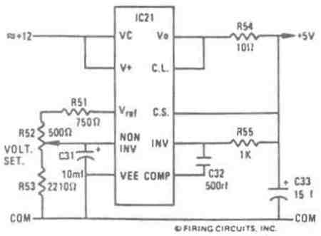
FIGURE 48. 1679/1681 DC MOTOR CONTROL.
CONNECTION OF LOGIC CIRCUIT POWER SUPPLY REGULATOR
3.4 Reference Voltage
The reference voltage for the motor speed control is obtained from a monolithic integrated circuit voltage regulator, as shown in figure 4. The integrated circuit contains a temperature compensated voltage reference of approximately 7 volts, an error amplifier, a series pass transistor, and a current limiter, as shown in figure 4A. The compensated reference is attenuated, to 5 volts by Resistors R51, Potentiometer R52, and R53, as shown in figure 4B. The attenuated reference is connected to the non-inverting input of the error amplifier. The error amplifier compares the 5 volt reference signal with the regulator output voltage. The amplified error signal controls the series pas s transistor to maintain 5 volts at the regulator’s output. However, an abnormal current flow in external Resistor R54 will turn the current limiting transistor on and reduce the signal to the base of the series pass transistor. Reducing the base signal reduces the output voltage, thereby protecting the regulator against accidental short circuits or shorted logic components.
3.5 Minimum Speed Circuit
The minimum speed adjustment is buffered by a unity gain amplifier as shown in figure 5. Its adjustment range is zero to approximately 20% of full speed.
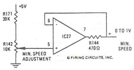
FIGURE 5. 1679/1681 DC MOTOR CONTROL.
MINIMUM SPEED CIRCUIT
The minimum speed adjustment may alternately be used as an offset adjustment. Figure 6A shows the connection for “minimum speed” adjustment. The variable output from IC27 is added to the speed adjust potentiometer, providing a bottom limit to the speed setting.
Figure 6B shows the connection for “offset” adjustment. The variable output from IC27 is connected to the non-inverting input of input amplifier IC23. This provides an offset signal to compensate for speed corrunand devices with minimum outputs higher than zero.
3.6 Electronic Mode Selector Switch
The mode selector circuit, shown in Figure 7, is used to switch between the acceleration/deceleration mode, inch mode, and jog mode. In the normal acceleration/deceleration connection, the run enable signal is high (+5V), switch “C” is on, and the speed commands come from the speed control potentiometer through the acceleration/deceleration ramp. However, this input may also be used for a “speed follower” input signal, when the ramp is not required or desired. In the inch mode, the inch adjustment potentiometer is connected directly to the speed command amplifier through switch “B” without an acceleration/deceleration ramp. The inch mode is selected by applying a logic 1 (+5V) to the inch enable input. Selection of the jog made by applying a logic I (+5V) to the jog enable input, connects the jog adjustment potentiometer directly to the speed command amplifier via switch “A”. Usually the jog adjustment potentiometer is preset to the desired jog speed and the jog enable input is used to jog the motor.
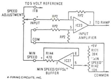
FIGURE 6A. 1679/1681 DC MOTOR CONTROL.
MINIMUM SPEED CIRCUIT CONNECTIONS
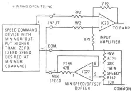
FIGURE 68. 1679/1681 DC MOTOR CONTROL.
CONNECTION FOR OFFSET ADJUSTMENT
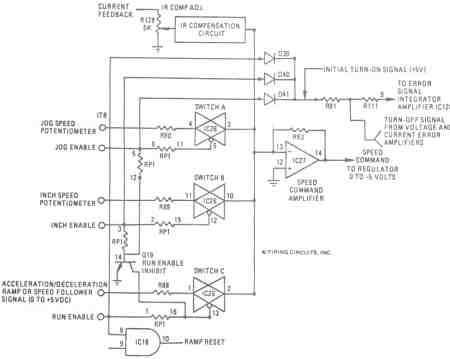
FIGURE 7. 1679/1681 DC MOTOR CONTROL.
ELECTRONIC MODE SELECTOR SWITCHES
The mode selector circuit has three other functions of interest. The first is a “run enable inhibit” function. If either the inch or jog enable circuit is energized, a signal appears on the base of Transistor 019. When 019 conducts, the enable terminal (13) of enable switch C of IC 26 is clamped to ground, preventing the turn on of the run circuit. The second function is a ramp reset action, from the run enable circuit. When the run enable circuit is energized, a “Logic I” (+5V) signal is sent to NAND gate IC18, causing the ramp to reset. This prevents “bumping” the drive if the drive is turned on before the deceleration ramp has reached a low value.
The third function causes each enable circuit, through Diodes D39, d40, and D41. to provide a turn-on signal to the high gain error-integrating amplifier IC28. The purpose of this circuit is to provide fast control response to turn-on commands. and to eliminate effects of amplifier offset at the operating speed.
3.7 IR Compensation
IR compensation is combined with the speed signal at the speed command amplifier. as shown in figure 7. IR compensation adjustment range is zero to approximately 20% boost.
The IR compensation circuit automatically proportions the compensating signal to armature voltage, so that the compensation is essentially constant over the entire speed range.
3.8 Speed Regulator
The speed regulator circuit is shown in figure 8. It consists of four operational amplifiers that function as a speed error amplifier, current error amplifier, regulator, and level shifter respectively.
The speed and current error amplifiers function together to supply an error signal to the speed regulator. When the motor current level is below the current limit level, the current error amplifier ICZ8 is at its positive voltage limit and the motor armature voltage or speed error amplifier is supplying the error signal to the regulator. However, if the current limit is exceeded, the current error amplifier will take control of the regulator.
The voltage and current error amplifiers have fast response times and relatively low gains. The ;regulator amplifier has a high gain but relatively slow response. This arrangement produces a motor control with a quick responding current limit while maintaining good stability and excellent speed regulation.
The level shifter amplifier inverts the zero tb minus five volt regulator signal to a plus five to zero volt signal. The plus five to zero voltage signal controls the voltage controlled oscillator (clock) frequency in the digital gating circuit.
With a command signal, from a potentiometer or external command device, applied to the “external current limit” input to the current error amplifier ICZ8, the control becomes a cur rent control amplifier. The current command signal can be brought through the acceleration/deceleration ramp circuit, or directly to the speed command circuit. No internal potentiometer is provided for this function.
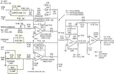
FIGURE 8. 1679/1681 DC MOTOR CONTROL.
SPEED REGULATOR CIRCUIT
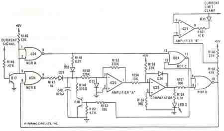
FIGURE 9. 1679/1681 DC MOTOR CONTROL.
INITIAL STARTING CURRENT TIMER
3.9 Initial Starting Current Timer
The maximum current limit value is higher for starting then for running (200% start and 150% run). The circuit t hat permits the higher starting current is shown in figure 9. Initially, the output of NOR gate D is high (+5V), 5V is applied to amplifier “B” and the reference voltage
When the current starts to flow, transistor Q17 turns on. The output of NOR gate “A” switches to a logic high, NOR gate “C” switches low, transistor Q18 turns off and capacitor C49 charges through R148 and D32. The capacitor voltage is inverted by amplifier “A” and compared with a fixed level at the comparator. The capacitor charges until its voltage level causes the comparator to switch positive, after approximately 5 seconds. The positive voltage from the comparator causes NOR “D” to switch to a logic zero (0V). A logic zero from NOR “D” attenuates the voltage applied to amplifier “B”. This reduces the reference voltage for the current limiter to approximately 3.3V corresponding to 150% of rated current.
When current stops flowing, transistor Ql7 turns off, NOR “A II and NOR “B” switch low and capacitor C49 starts to discharge through R1SO and D33. After approximately three minutes of discharge, the comparator switches low, the NOR gate “D” switch high and the current limiter’s reference voltage returns to 5V, or 200% of rating.
3.10 Isolation Circuit
The armature current and voltage signals are isolated from the control circuit as shown in figure 10. The current and voltage signals are modulated or chopped by an electronic chopper, transformer coupled, and demodulated to produce isolated signals.
The chopper consists of an operational amplifier and an electronic switch. The operational amplifier has a gain of plus one when the switch is off and minus one when the switch is on, as shown in figures 11 and 12. Switching between plus and minus gains modulates the signal to produce an AC signal (et in figure 12) at the transformer. The modulated signal is transformer coupled to the output amplifier. The output amplifier is synchronously switched between a plus one and minus one gain to demodulate the signal. The output amplifier is in effect a synchronous rectifier. The current signal isolator output is also brought to terminal TB2, to provide a signal proportional to armature current, but isolated from armature voltage.
3.11 Firing Circuit
The function of the firing circuit is to sequentially turn on each thyristor at the proper time. This is accomplished by detecting a reference point with the applied voltage cycle and initiating a firing pulse train after the proper delay time.
It can be seen from figure 13, that the “on” time of the thyristor is increased by decreasing the delay time and vice-versa. It follows that the output power can be varied by changing the delay time. The delay time is obtained from a fixed length electronic counter, counting pulses from an electronic clock. The clock is a voltage controlled oscillator. When the clock is at a low frequency, more time is required for the counter to reach its preset count, hence there is a long delay. If the clock frequency is high, the counter needs less time to reach the required count.
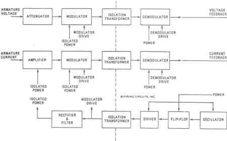
FIGURE 10. 1679/1681 DC MOTOR CONTROL.
BLOCK DIAGRAM OF ISOLATION CIRCUIT
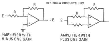
FIGURE 11. 1679/1681 DC MOTOR CONTROL.
INTRODUCTION TO ISOLATION CIRCUIT
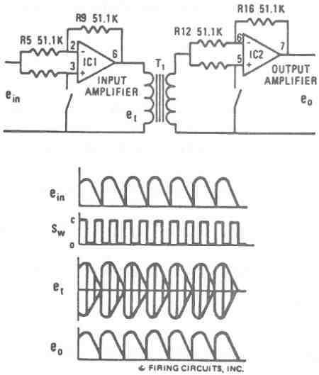
FIGURE 12. 1679/1681 DC MOTOR CONTROL.
ISOLATION CIRCUIT, MODULATOR-DEMODULATOR
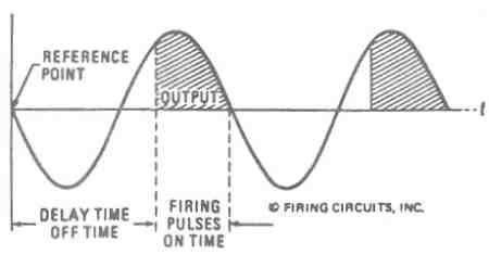
FIGURE 13. 1679/1681 DC MOTOR CONTROL.
FUNCTION OF FIRING CIRCUIT
When the counter has obtained the required coWlt, meaning the required delay has passed, and assmning no fault conditions exist, an electronic gate opens, allowing firing pulses to turn on the thyristor. The firing pulses are removed after 1200, or at the next crossing of the timing reference point, whichever occurs first. The coWlter is always reset at the reference point crossing. Figure 14 is a simplified block diagram of a three SCR, three diode motor control. Figure 15 shows a six SCR motor control. Each SCR has its own reference detector and counter. The coWlters work off a common clock signal to assure virtually identical delay times for each SCR firing. Independent referencing detectors allow the angle between phases of the line to vary (phase shift) without effecting the firing angle.
3.11.1 Clock (Voltage Controlled Oscillator)
A simplified block diagram of the clock or voltage controlled oscillator is shown in figure 16. The Capacitor C charges at an exponential rate which is set by Resistors RA, RB, and Capacitor C. When the ‘capacitor voltage reaches the control voltage, the threshold comparator triggers the flip-flop so that its output is set high. This sets the clock’s output low and turns on the discharge transistor, allowing the capacitor to discharge through Resistor RB. When the capacitor discharges to half the control voltage, the trigger comparator triggers the flip flop so that its output is set low. This turns the capacitor discharge transistor “off” and drives the clock output high. The capacitor starts to charge again and the cycle repeats.
The capacitor voltage oscillates between the control voltage and half the control voltage. Increasing the control voltage will increase the magnitude of the oscillation and the time required to complete a cycle. Hence, increasing the control voltage will decrease the frequency of oscillation and vice-versa.
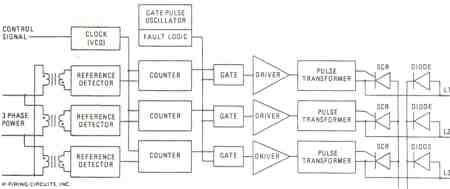
FIGURE 14. 1679/1681 DC MOTOR CONTROL.
SIMPLIFIED 8LOCK DIAGRAM OF A 3 SCR, 3 PHASE DIGITAL FIRING CIRCUIT
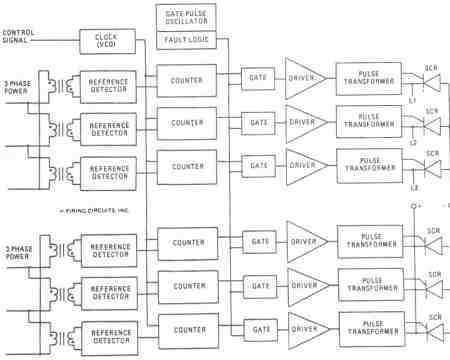
FIGURE 15. 1679/1681 DC MOTOR CONTROL.
SIMPLIFIED 8LOCK DIAGRAM OF A 6 SCR, 3 PHASE DIGITAL FIRING CIRCUIT
3.11.2 Reference Detectors
Each reference detector locates a reference point on the input voltage cycle and generates a timing pulse. The reference point is very close to the negative zero crossing, since this allows full variation of output power with minimum variation of delay time.
The circuits that develop the reference or reset pulses are shown in figure: 17 and figure 18. The circuit of figure 17 simply conditions the line voltage, while the circuits in figure 18 develops the actual pulses.
Each phase of the three phase line voltage is transformer coupled into a low pass filter which removes transients and noise. The output of each filter is amplified and clipped to produce square waves. The square waves convey zero crossing information to the reference pulse circuits of figure 18 and the phase sequence circuit, figure 22.
The three square waves are connected to the twelve monostable multivibrators which produce six reference pulses displaced 600 from one another as shown in figure 18. Each reference pulse resets one of the six electronic counting circuits. Note: a three SCR. three diode motor control requires only six multivibrators and
three reference pulses displaced 120°.
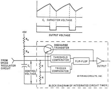
FIGURE 16. 1679/1681 DC MOTOR CONTROL.
VOLTAGE CONTROLLED OSCILLATOR (VCO)
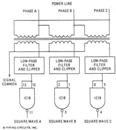
FIGURE 17. 1679/1681 DC MOTOR CONTROL.
AC LINE FILTER & CLIPPER
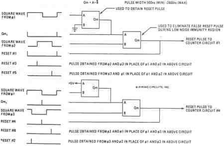
FIGURE 18. 1679/1681 DC MOTOR CONTROL.
DEVELOPMENT OF RESET PULSES IN TRIGGER CIRCUIT
3.11.3 Counting Circuit
A typical counting circuit is shown in figure 20, with its timing diagram in figure 19. The. zero crossing of the line voltage resets the counter, to start the timing cycle. The first part of the timing cycle corresponds to the SCR off time and lasts for 1000 clock pulses, on a 60Hz system (1200 for 50Hz systems). After counting a 1000 (1200) clock pulses, the counter output (QlB of counter “B”) switches to a logic “1” (+5V), and allows the firing pulse produced by the gate pulse oscillator to pas s through the NAND and NOR gates of figure 20. The firing pulse out of the NOR gate is amplified by the two transistors, and transformer-coupled to the SCR gate with which it is associated.
The number of gate pulses and the manner by which they are removed depend on the output level of the motor control. For low output levels, small conduction angles, the SCR receives gate pulses until the counter is reset by the next zero crossing. However, at high output levels, the gate pulses are inhibited by the NOR gate after 120 electrical degrees, since the SCR is commutated off at this point and further gate pulses would simply cause gate heating.
3.11.4 Gate Pulse Oscillator
The SCR firing pulses are generated by the gate pulse oscillator, sh own in figure 21. NAN? gate “A” and “B” form an oscillator which is synchronized by the NOR gate “A” and “B” at the turn on of each SCR. The synchronization circuit is designed to produce a wide initial firing pulse, which increases accuracy of the firing angle, and adds to the DI/DT capability of the SCR.
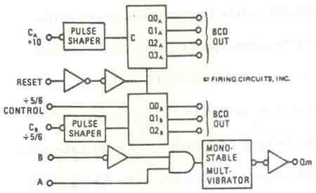
FIGURE 19. 1679/1681 DC MOTOR CONTROL.
COUNTER :TIMING DIAGRAM
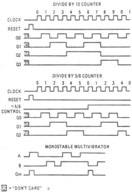
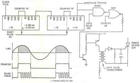
FIGURE 20. 1679/1681 DC MOTOR CONTROL.
COUNTER AND GATE PULSE CIRCUIT
Gate pulses can only pass through NAND “c” if the phase sequence and phase 1088 circuits determine that the correct power is present. Likewise, NOR “c” only allows pulse passage when the control is enabled and no fault condition is detected.
3.12 Fault Protection Circuits
The fault protection circuitry senses several different circuit conditions and inhibits thyristor gating in the event these conditions become harmful to the system.
The following is a list of conditions which will inhibit operation:
- hnproper phasing of input voltage
- Loss of an input phase voltage
- Excessive load current
- Over-temperature of heat sink as sembly
- Opening of interlock circuit
3.12.1 Phase Sequence and Phase Loss
Correct phase sequence of the incoming power lines is necessary for proper thyristor firing. Therefore, the fault logic circuits contain a phase sequence detector to prevent incorrect operation.
If the incoming phase sequence is not ABC, the phase detector will inhibit thyristor firing and no power will be supplied to the motor. Incorrect phasing is corrected by reversing any two input power lines.
The phase detector is shown in figure ZZ. Squared-off phase voltage signals are fed to it from the line filter circuit (figure 17). When the phase sequence is correct (ABC), the positive and negative phase signals directly coupled to each NAND gate and the capacitor coupled positive leading edges and negative trailing edges of the preceeding phase signal are opposite polarity. The output of the NAND gates therefore remain high, allowing gate pulses to flow to the SCR IS. However, if the sequence is incorrect (ACB), the directly coupled input signals and the leading and trailing edges of the capacitor coupled input signals are in the same polarity, causing the NAND gate to pulse low. These low pulses discharge the capacitor C20, which inhibits the gate pulse oscillator.
Loss of an input phase also results in direct and capacitor coupled pulses to be in phase, causing the NAND gate to pulse low. The pulses keep capacitor C20 discharged, thereby inhibiting the gate pulse oscillator.
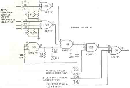
FIGURE 21. 1679/1681 DC MOTOR CONTROL
GATE PULSE OSCILLATOR
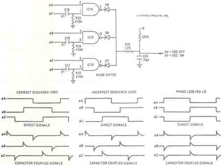
FIGURE 22. 1679/1681 DC MOTOR CONTROL
PHASE SEQUENCE CIRCUIT
3.12.2 Over- Temperature and Interlock
Thermal overload protection protects the thyristors from operation beyond their temperature limit. Without this protection, high ambient temperatures or high continuous power overloading could produce excessive thyristor temperatures. A bi-metal temperature switch mounted on the heat sinks accomplishes this protection.
The over-temperature protection circuit is also shown in figure 23. If an over-temperature condition occurs, one or more of the thermal switches will open. Opening a thermal switch will set the latch to a logic “1”, remove the gate pulses and turn on the fault trip LED. This inhibits the controller until it is reset.
NOTE: The controller will not reset until bi-metal switch has cooled enough to allow the contacts to reclose.
External interlock devices (normally closed) may be connected into this circuit between terminals ITBI and ITB2, as shown on the installation drawing.
Opening the external interlock shuts the controller off in the same manner as the thermal overloads.
After the fault condition is corrected, the reset command will reset the latch, enable the gate pulse oscillator, and resets the analog control circuits. The control circuits will not restart the motor until the reset command is removed.
3.12.3 Current Trip
An excessive peak current will cause the output of the current trip amplifier to switch negative. This sets the latch in figure 23 to a logic 1, removes the gates pulses and turns on the fault trip LED. Depressing the reset will clear the latch and turn off the LED.
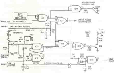
FIGURE 23. 1679/1681 DC MOTOR CONTROL.
TRIP CIRCUIT
Starr-Up Procedures
- STAR T UP PROCEDURES
The following steps and procedures should be followed closely to insure proper operation of the motor controller.
4.1 Mechanical Installation
Since in most cases the motor control is previously installed in an enclosure, only a quick mechanical check is necessary. Check mounting hardware holding the controller base to the enclosure.
Open the front panel and check that all circuit boards are in place. Be sure all circuit cards are firmly in place. The location of the controller apparatus should be a reasonably clean, dry environment. Ambient temperature around the system should be such that the temperature inside the controller enclosure does not exceed 50°C.
4.2 Electrical Installation
Before programmed inputs are made to the motor controller, an operational check is suggested, to confirm that the drive is functioning properly.
Refer to the Installation Drawing:
| 1679 Control: | 1679-4003, sheets 1 and 2 |
| 1681 Control: | 1681-4003, sheets 1 and 2 |
Sheet 1 of the Installation Drawing shows the connections for a standard drive, with a single speed adjust potentiometer to control motor speed from a minimum speed, as determined by the minimum speed control setting, to a maximum speed, as determined by the minimum speed control setting. Connections arc shown for either armature voltage feedback regulation, or tachometer generator speed regulation. The tachometer generator feedback circuit is designed for a 5 volt DC signal at maximum generator speed. If the generator output exceeds 5 volts, a voltage divider network is needed to reduce the voltage to the 5 volt level. The voltage divider, its connection, and the formula for calculating the resistors is shown on the Installation Drawing. An AC tach generator may be used if its output is rectified and filtered. Ripple voltage should not exceed one percent at any point in the speed range. However, the ripple filter may cause response or stability problems.
Sheet 2 of the Installation Drawing shows typical connections for other uses of the control. For jogging or inching, the speed adjustment potentiometers are shown connected to apply the speed signal into one of the direct inputs, without going through the ramp circuit. This is to produce crisp action when the jog or inch button is pressed. The jog connection is shown for about a zero to 50 percent adjustment range. For a lower maximum jog speed, increase the value of the fixed series resistor and decrease the value of the jog potentiometer the same amount.
For “offset” control, to compensate for an instrument or other speed follower signal that has a residual output at minimum (such as 5 to 50 milliamperes), the minimum speed amplifier of the control is connected as shown. This connects the minimum speed amplifier to the non-inverting input of the input amplifier.
A typical connection is shown for connecting two controls with one as the lead, or master control, and the other as the follower, or slave. The speed signal into the follower control is connected to a direct input instead of through the ramp, to insure tracking of the drives during acceleration or deceleration. The connection shown does not provide for individual minimum speed adjustment, however. The minimum speed adjustment in the lead drive is common to both drives. The minimum speed circuit cannot be connected in both drives because the higher signal will over ride the lower one. Diode isolation cannot be us ed because of the low signal level. If individual minimum speed adjustment is needed for accurate system tracking, ‘a master reference supply with isolated 0 – 5 volt speed signals should be used. A less costly but less accurate alternative is the use of two ganged speed adjustment potentiometers, controlled by a single knob.
4.3 Checks Before Initial Start-Up
Ohmmeter Checks (DC Motor Disconnected)
- Check all power terminals and control terminals for grounds, using the X10 scale on the ohmmeter.
- Check between AC power terminals L1, L2, L3, on the Xl ohmmeter scale. Readings should be approximately 340 ohms. Check between plus and minus armature terminals on the X10 scale. On the 1681 control, reading should be meg ohms with meter in either polarity. On the 1679 control, reading should be megohms with plus of meter on plus armature terminal, very low resistance with opposity polarity.
- Check all motor leads (including tachometer and motor thermostat leads) for grounds, and for insulation integrity between the shunt field and armature circuit. It is advisable to use a megger for the motor insulation tests.
Check motor field resistance, and compare to nameplate data.
Voltage Checks (SEE WARNING, Section V)
- Connect jumper on regulator card for armature voltage feedback.
- If available, connect a light “dummy” load to armature terminals. A number of 200 watt light bulbs in series will do (three for 240 volts DC, six for 500 volts DC).
- Turn’ speed adjust pot to minimum.
- Apply AC power. Check AC line volts at terminals L1, L2, L3.
- Phase sequence LED indicator on regulator board should light. If it does not, SHUT OFF AC POWER, interchange any two AC power leads, reapply AC power.
- Push drive start or run button.
- Check armature output volts. With minimum speed adjustment on regulator board full CCW, should be close to zero. With minimum speed pot turned full CW should read approximately 20 percent of rated armature voltage. Reset minimum speed full CCW.
- Slowly turn speed adjust pot turns maximum. DC armature volts should increase to approximate rated value. Turn maximum speed adjustment on regulator board through its full range. Armature voltage should vary from approximately 100 percent rated volts to 120 percent rated volts. Return speed adjust pot to minimum.
- Check for correct DC motor field volts. In 1679 control, 300 volts or 150 volts DC fixed field supply can be obtained from the control, per connection indicated on the Installation Drawing. When the 1681 control is used, the field supply must be obtained from another source.
- If any of these checks indicate an abnormal condition, refer to section v – Trouble Shooting Procedure for additional check steps.
- When the control is checked out, Shut Off AC Power. Remove dummy load and connect motor leads. Adjust jumper on regulator board for correct feedback mode.
4.4 Trim Adjustment Settings
Adjustment of the trim pots located on the regulator card may be necessary of for the needs of your application.
Adjust trim pots as follows:
Trouble-Shooting Procedures
- TROUBLE-SHOOTING PROCEDURES
The following trouble-shooting guide (see page 40 ) should be referred to when operating difficulties occur.
The guide is broken down into three sections:
Symptom – description of problem
Probable Difficulty – description of what may be wrong
Check or Replace – action to be taken
This guide is also supplemented with a power module bench test. Ommeter readings are given as a check for faulty semiconductors.
The steps shown in the trouble-shooting guide should be followed before substitution of any modules.
TROUBLE SHOOTING
TYPE 1679 AND 1681 DC CONTROLS
| WARNING HIGH VOLTAGE Electric shock can cause serious or fatal injury. Whether the AC voltage supply is grounded or not, high voltages to ground will be present at many points within the SCR control. Extreme care must be exercised in the selection and use of test instruments. Operators should not stand on grounded surfaces or be in contact with ground when applying test instruments to test points. Test instruments should not have chassis grounded while test are being made. Extreme care should be taken during the use of test instruments such as an oscilloscope, since their chassis may be at high voltages with respect to ground during testing. |
In the event of malfunction, check the obvious but frequently
overlooked causes of trouble:
- Loose or broken connections. All terminals should be tight.
- Control devices and interlocks external to the control.
- Excessive1y high or low incoming AC voltage. Standard tolerance is + 10%.
- Atmospheric contamination can cause insulating films to develop on relay and push button contacts, expecia11y those in low energy circuits.
- Noisy power lines. Incoming supply may contain “high energy spikes” which can cause erratic operation.
- All scope or meter readings called for in the trouble-shooting chart are measured with respect to common, at terminal TB1-14.
| SYMPTOM | PROBABLE CAUSE | CHECK | REPAIR OR REPLACE |
| Phase sequence L.E.D. does not lite with power applied | Incorrect phase sequence | Interchange two incoming power lines. | |
| No power to control | Measure input at L1, L2, L3 | ||
| Blown power or control fuses | All fuses | Fuses | |
| Jumpers missing or not connected on Filter Board | Filter board | Install jumpers | |
| Filter board faulty | Check output of filter board with scope at TB2-1, TB2-2, TB2-3 * | Filter Board | |
| Control board faulty | With scope, check for 5.0 Volts from anodes of D7, D8, D9 | Control Board | |
| Control blows line fuses with power applied | SCR’s and power diodes | Check SCR’s and Diodes, MOV’s | SCR’s or Diodes, MOV’s |
| Faulty Motor | Motor field and armature (megger if breakdown is suspected after disconnecting from o | Motor | |
| Phase sequence L.E.D. lit no output from control with speed adjust full C.W. | No supply voltages | +5.0 volts from TB1-1 | Control or filter board |
| +12.0 volts from TB2-4 (filter board) | |||
| -12.0 volts from TB2-5 (filter board) | |||
| No reference voltage | +5.0 volts from TB1-13 | External speed adjust | |
| Current limit set full C.C.W. | Adjust current limit pot for 3.0 volts from TB1-12 | Control Board | |
| No run enable signal | +5.0 volts from TB1-7 external enable contacts | External enable contacts or control board | |
| No ramped output | +5.0 volts from TB1-10 | Control Board | |
| Open Jumper | Connection diagram | Jumper | |
| “M” contacts faulty power or aux. | Contacts | “M” Contactor or “run” relay. | |
| Gating & Isol. Board | Check pulse train with scope * | Gating & Isol. Board | |
| Phase sequence L.E.D. lit, fault L.E.D. lit, no output from control | Open interlock or heatsink thermostat open | +5.0 volts from TB1-2 | Interlock or Thermostat |
| Overcurrent trip (I.O.T.) | Excessive load condition, short circuit in motor or motor leads intermittent short in motor, SCR breakover, megger SCRs (out of circuit). |
Check machine & processes Check motor. Replace SCRs with low, megger readings. |
|
| Motor runs at base speed or higher with low reference voltage applied. | Jumper missing or in wrong mode in control board. | Jumper A to T for arm. feedback. Jumper T to T for tach feedback. | Reconnect or install jumper |
| Defective tachometer or coupling | Tach output | Tachometer or coupling | |
| Defective feedback isolator | +2.25 volts from terminal A on control bd. at 500 volts output | Isolation & gating board | |
| Defective control board | TP-10 control bd. for +4.0 volts | Control Board | |
| Control starts but will not reach max. speed with speed adjust full C.W. | Max. speed set too low | Adjust max. speed | Control Board |
| Current limit set too low | Adjust current limit | Control Board | |
| Reference voltage | +5.0 from TB1-13 | Control board, Power Supplies (Filter board) | |
| Jumper in wrong mode on iso. & gating board | Jumper 1 to 2 for 500 volts Jumper 2 to 3 for 240 volts |
Jumper for correct arm. voltage | |
| Control will not regulate speed with load | Current limit set too low | Adjust current limit setting +3.0 volts TB1-12 | Control Board |
| Incorrect ammeter shunt | Shunt | Install correct shunt | |
| Current isolator defective | Load current TB2-1 for 1.25 volts @ 100% load. | Isolation & gating board | |
| Line voltage drooping with load | Line voltage when load is applied, voltage should not droop more than 10% | Check AC supply for adeqacy and/or loose connections. | |
| Overload condition | Load current | Correct cause of overload | |
| Control Unstable | Stability or forcing not properly adjusted | Control Board | Adjust “stability” and “forcing”. Replace board |
| Ammeter shunt signal leads reversed | Check lead polarity | Connect leads correctly | |
| Defective tachometer or coupling | Tachometer and coupling | Tachometer or coupling | |
| Motor or load binding up | Load | Correct load condition | |
| Speed amplifier | Control bd., IC25, IC27 | Control board | |
| Voltage isolator defective | Voltage isolator 2.25 volts from terminal A on control board @ rated arm. voltage | Isolation & gating board | |
| Reference voltage unstable | TB1-13 for stable volt. level | Control bd. or external po | |
| Current limit set too low | Current limit setting (speed wil rise as soon as it is turned to higher current set. | Correct current limit setting | |
| Wrong ammeter shunt | Ammeter shunt | Install correct shunt | |
| Control bd. defective | Control bd. (substitue spare board) | Replace control board | |
| * See schematic for waveforms. |
POWER MODULE BENCH TEST
The purpose of this test is to determine whether the power module being tested has a defective thyristor, or thermal sensing switch.
Remove the module from the base panel and lay on its side. At this point it will be helpful to refer to the “Exposed View of the DC Motor Controller” at end of manual. The upper portion of the picture shows in detail the parts of the SCR/SCR power module.
Use a Simpson type 270 Multimeter or equivalent and set the meter to ohms Rx 1 or RxIO.
Thyristor Check
Connect (+) of ohmmeter to SCR cathode test jack, (-) of ohmmeter to SCR anode test jack. Meter should read open. Reverse the ohmmeter leads. Ohmmeter should again read open.

Now place (+) ohmmeter lead on gate test jack, (-) lead on anode test jack. Ohmmeter should read open. Reversing leads should again give an open reading. Connect (+) of ohmmeter to gate test jack, (-) of ohmmeter to cathode test jack. Ohmmeter should read between Ion and 300n. Reverse ohmmeter leads. Meter should now read between 20n and soon.
Thermal Sensor Check
Connect leads of ohmmeter to the two terminal tabs located on the thermal sensor. The ohmmeter should read zero ohms.