![]()
Switching Bus With IGBTs
Today’s inverters use Insulated Gate Bipolar Transistors (IGBTs) to switch the DC bus on and off at specific intervals. In doing so, the inverter actually creates a variable AC voltage and frequency output. As shown in Fig. 7, the output of the drive doesn’t provide an exact replica of the AC input sine waveform. Instead, it provides voltage pulses that are at a constant magnitude.
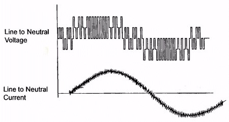
Figure 7, Drive Output Waveform
The drive’s control board signals the power device’s control circuits to turn “on” the waveform positive half or negative half of the power device. This alternating of positive and negative switches recreates the 3 phase output. The longer the power device remains on, the higher the output voltage. The less time the power device is on, the lower the output voltage (shown in Fig.8). Conversely, the longer the power device is off, the lower the output frequency.
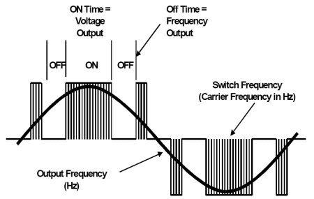
Figure 8, Drive Output Waveform Components
The speed at which power devices switch on and off is the carrier frequency, also known as the switch frequency. The higher the switch frequency, the more resolution each PWM pulse contains. Typical switch frequencies are 3,000 to 4,000 times per second (3KHz to 4KHz). (With an older, SCR (Silicon Controlled Rectifier)-based drive, switch frequencies are 250 to 500 times per second). As you can imagine, the higher the switch frequency, the smoother the output waveform and the higher the resolution. However, higher switch frequencies decrease the efficiency of the drive because of increased heat in the power devices.
Shrinking cost and size
Drives vary in the complexity of their designs, but the designs continue to improve. Drives come in smaller packages with each generation. The trend is similar to that of the personal computer. More features, better performance, and lower cost with successive generations. Unlike computers, however, drives have dramatically improved in their reliability and ease of use. And also unlike computers, the typical drive of today doesn’t spew gratuitous harmonics into your distribution system-nor does it affect your power factor. Drives are increasingly becoming “plug and play.” As electronic power components improve in reliability and decrease in size, the cost and size of VFDs will continue to decrease. While all that is going on, their performance and ease of use will only get better.
Study on design and fabrication of insulated gate bipolar transistor
Abstract
Power Bipolar Transistor and Power MOSFET are the most commercial advanced devices. Each device has characteristics that complement each other in some respects. Power Bipolar Transistors have lower conduction losses in the on-state, larger blocking voltages, but low switching speed. In contrast Power MOSFETs can switch faster, but conduction losses in on-state are higher. Nowadays, the new structure has been designed in order to overcome to the performance limitations of Power Bipolar Transistor and Power MOSFET. Such the device is know as the Insulated Gate Bipolar Transistor (IGBT). This device has significant superior characteristics for low and medium frequency applications compared to Power Bipolar Transistors and Power MOSFETs. Furthermore, its power rating can be improved by increasing both current and voltage. For this reason, this device more preferable over Power Bipolar Transistors and Power MOSFETs in many electronic systems and applications. The design, the fabrication process, the packing assembly and the experimental results of discrete planar and vertical IGBT are studied and reported in this thesis. The device is fabricated by using the double diffusion technique N/P+ type silicon epitaxial initial wafers. With the combination of MOS gate structure and bipolar current conduction, the IGBT structure can give not only a very high input impedance but also the high operating forward current density. However, on the other side, such a structure has a parasitic P-N-P-N thyristoe occurs between its collector and emitter terminals. This parasitic structure causes the latch-up effect in IGBT that makes the current to be no longer controlled by the MOS gate. This research begins with a study on parameters that can affect current conduction capability, on-resistance, breakdown voltage and switching speed.